Material | Process Applied | Dimension | Target Thickness | TTV | Rough. Sa. | ||
|---|---|---|---|---|---|---|---|
(inch) | (micron) | (micron) | (nm) | ||||
| Silicon Carbide | Rough Grinding | 6 | 150 | 2.472 | 1.420 | |
| Silicon Carbide | Wax Bonding | 6 | 200 | 2.648 | 0.193 | |
| Gallium Nitride | Rough Grinding | 4 | 300 | 2.181 | 0.963 | |
| Germanium | Rough Grinding | 4 | 145 | 2.905 | 0.256 | |
| Sapphire | Wax Bonding | 4 | 400 | 2.315 | 0.938 | |
| Gallium Arsenide | Back Taping | 4 | 55 | 2.240 | 5.062 | |
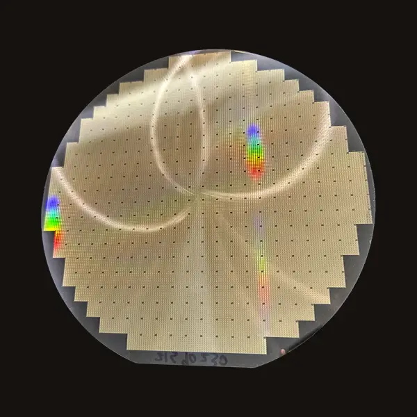
| Silicon | Rough Grinding | 12 | 300 | 2.782 | 10.065 | |
| Piezo Ceramic | Wax Bonding | 2 | 50 | 1.651 | 32.468 | |
| Silicon | Rough Grinding | 8.839 (M4) | 110 | 3.188 | 13.427 | |
| Silicon | Taiko Rough Grinding | 12 | 50 | 0.887 | 4.361 | |
| Silicon | Rough Grinding | 4 | 5 | 0.654 | 2.695 |

Material | Application | Process | Dimension | Flatness | Parallelity | Rough. Sa. | |
|---|---|---|---|---|---|---|---|
(mm) | (micron) | (micron) | (nm) | ||||
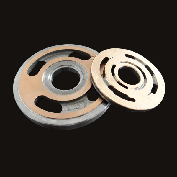
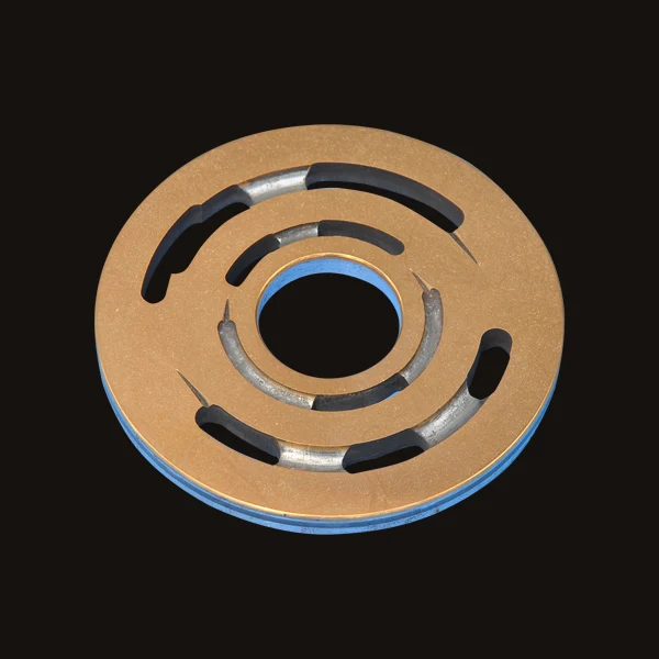
| Coated Cooper | Valve Plate | Lapping | Φ148×8 | 1.974 | 16.021 | NR |
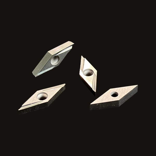
| Tungsten Carbide | Machining Bits | Lapping | Various | 1.243 | NR | NR |
| Stainless Steel | Slide Seal | (convex) | 36×6×5.5 | 1.695 | NR | 8.662 |
| Plated Gold | IC Package | Grinding | 240×96×2.35 | 3.493 | 34.746 | NR |
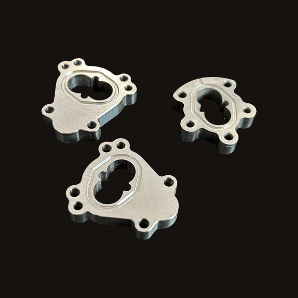
| Aluminum | Pump Plate | Lapping | Φ36.6×7.95 | 1.562 | NR | NR |
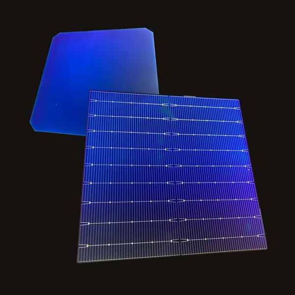
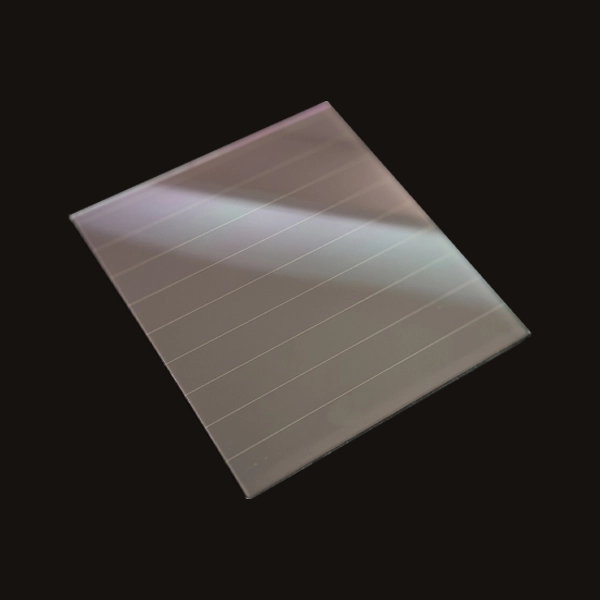
| Glass | Solar Panel | Lapping | 120×120×4 | 2.315 | 9.258 | 12.748 |
| Titanium Alloy | Aero Engine | Lapping | Φ862×522 | 7.515 | NR | 18.193 |
| Stacked Glass | Holographic | Lapping | Φ685×22 | 10.3 | 47.521 | 5.466 |
Material | Application | Process | Dimension | Flatness | Parallelity | Thick. Vari. | Rough. Sa. | |
|---|---|---|---|---|---|---|---|---|
(mm) | (micron) | (micron) | (micron) | (nm) | ||||
| Alumina | Air Seal Ring | Lapping | Φ82×5.5 | 1.487 | 1.653 | 4.841 | NR |
| Stainless | Automotive | Lapping | Φ80×4.75 | 2.347 | 2.815 | 5.642 | 16.374 |
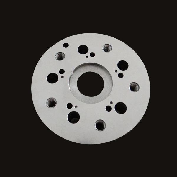
| Stainless | Pump Plate | Lapping | Φ232×47 | 1.775 | 2.656 | 4.147 | NR |
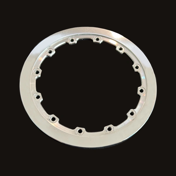
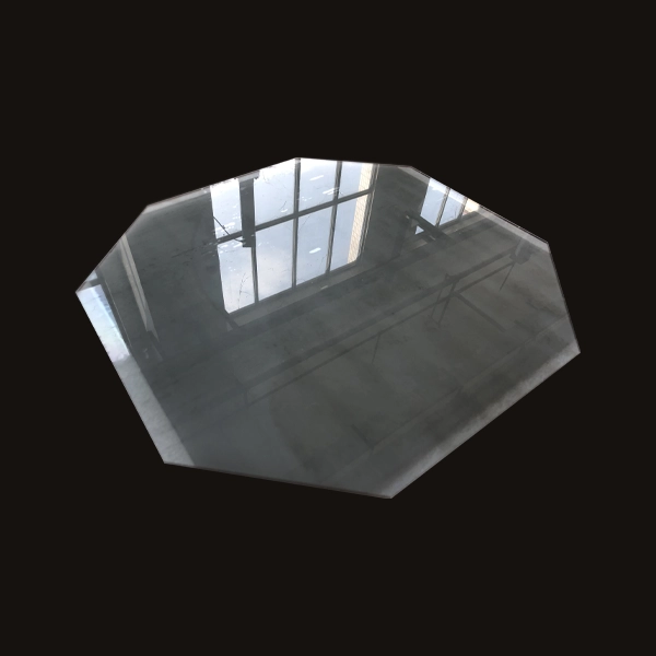
| SUS 304 | Valve Plate | Lapping | Φ173×8 | 2.886 | 3.132 | 8.667 | NR |
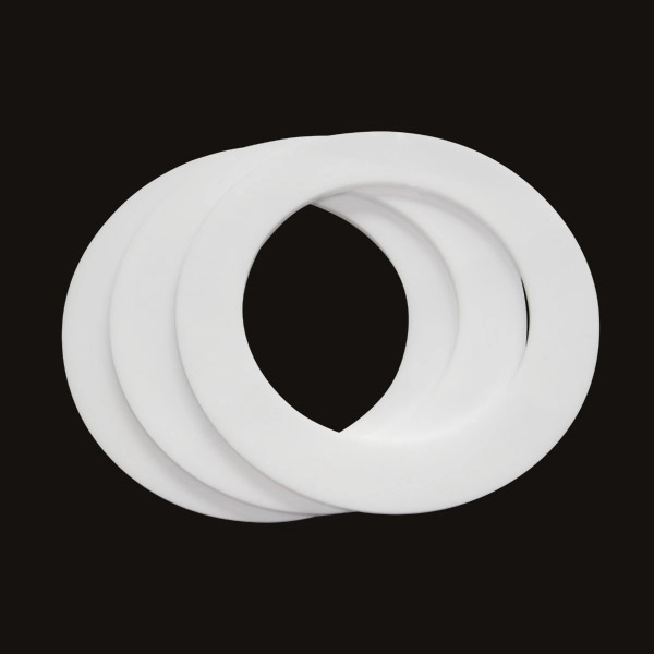
| Polyurethane | Valve Pad | Lapping | Φ260×0.77 | 2.835 | 2.989 | NR | NR |
| Carbide | Pump Hatch | Lapping | Φ103×4.05 | 1.823 | 2.138 | 1.985 | NR |
| Zirconia | Fingerprint | Lapping | Φ52×0.8 | 1.583 | 1.973 | 2.112 | 4.349 |
| Aluminum | Gauge | Lapping | 33×18×6 | 0.313 | 0.524 | 0.749 | 12.845 |