
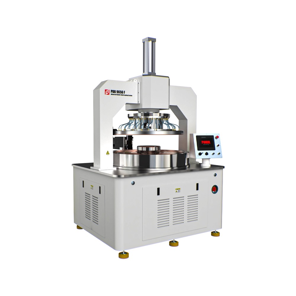
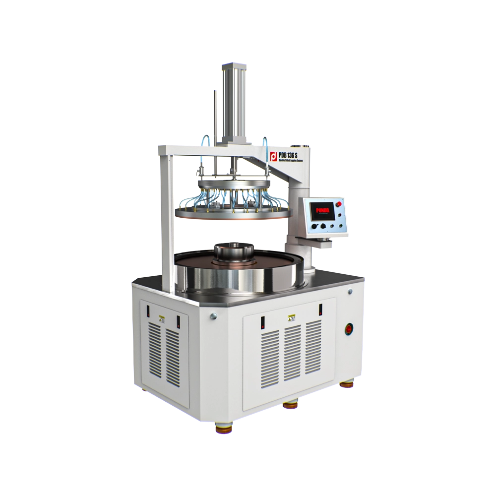
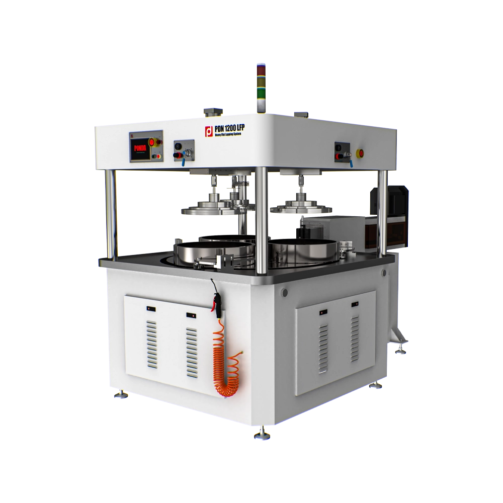
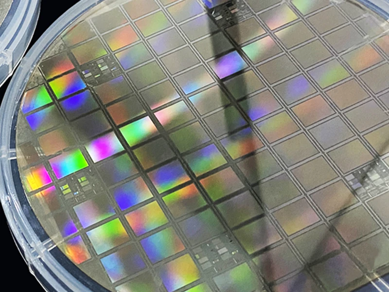
What can we do in Semiconductor industry?
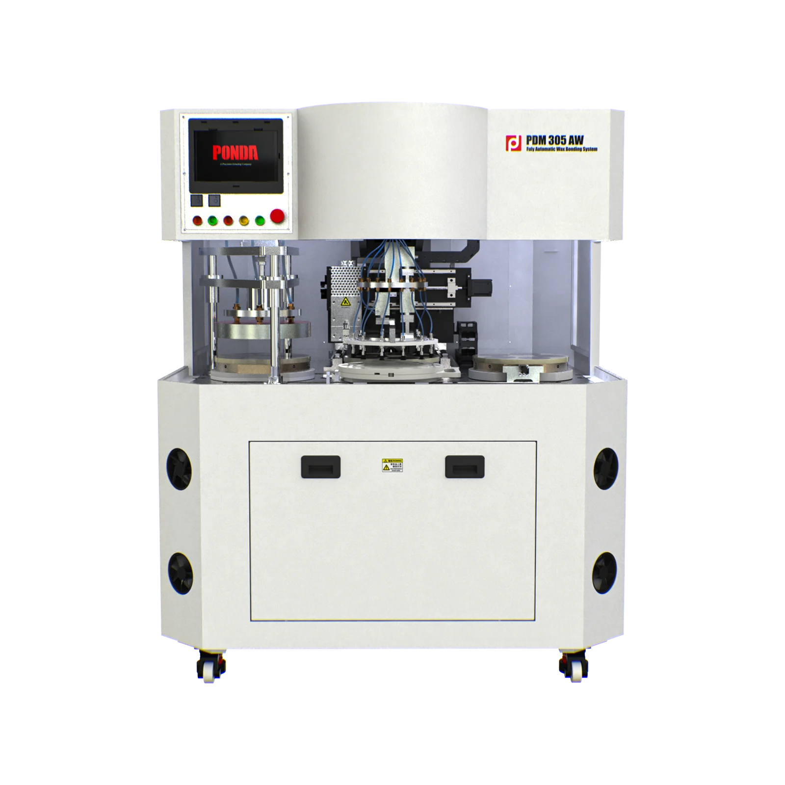
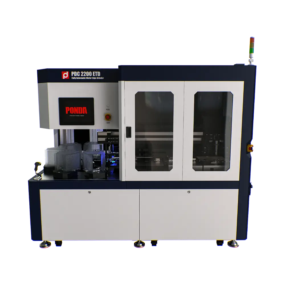
DYAN Grinding's machines provide key solutions in the semiconductor fabrication process, including wafer thinning, planarization, edge grinding, wax mounting, and surface finishing. These machines ensure precision at each step, helping to improve the quality and reliability of semiconductor devices. DYAN's equipment is designed to support various stages of semiconductor manufacturing, from thinning wafers to achieving smooth and uniform surfaces, contributing to more efficient production processes.
Applicable Processes
Process: Thins the wafer to a desired thickness by grinding. This is critical in applications such as wafer-level packaging, 3D ICs, and reducing die size for high-performance chips.
How it Helps: Ensures uniform wafer thickness, improving the overall quality and yield in semiconductor production.
Process: Chemical Mechanical Planarization (CMP) and lapping to achieve a flat surface. This is vital for ensuring smooth surfaces for photolithography and subsequent layers of semiconductor devices.
How it Helps: Ensures flatness and consistency across the wafer surface, which is essential for the fine-line patterning in photolithography.
Process: Grinds the edges of the wafer to remove rough edges and improve the uniformity of the wafer for easier handling in further stages, such as wafer dicing.
How it Helps: Reduces defects in the dicing process and ensures that wafer edges do not damage delicate components during handling.
Process: Mounts wafers using wax to provide temporary bonding during grinding and thinning. This prevents wafer breakage and cracks during the thinning process.
How it Helps: Protects wafers from damage during processing and ensures they remain stable for subsequent operations.
Process: Used for planarizing and polishing the wafer surface after grinding. These machines provide precise, uniform polishing, which is critical in the production of high-performance semiconductor devices.
How it Helps: Achieves the ultra-smooth surface required for advanced semiconductor applications, ensuring better device performance.
Process: After metal layers are deposited onto the wafer (such as copper or aluminum for interconnections), CMP is used to polish and planarize these layers to ensure even thickness.
How it Helps: Ensures that the metal layers are smooth, uniform, and free from defects, which is essential for reliable electrical connections in semiconductor devices.
Process: Achieves ultra-smooth, mirror-like finishes on the wafer surface.
How it Helps: The polished surface ensures optimal performance, especially in optoelectronic devices and components that require high surface quality, such as LEDs, lasers, and sensors.