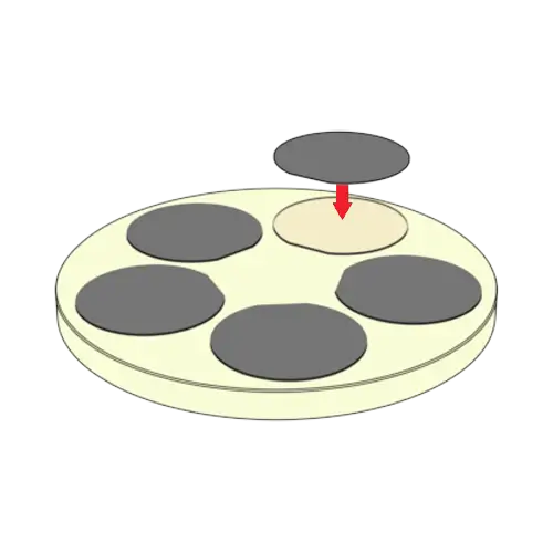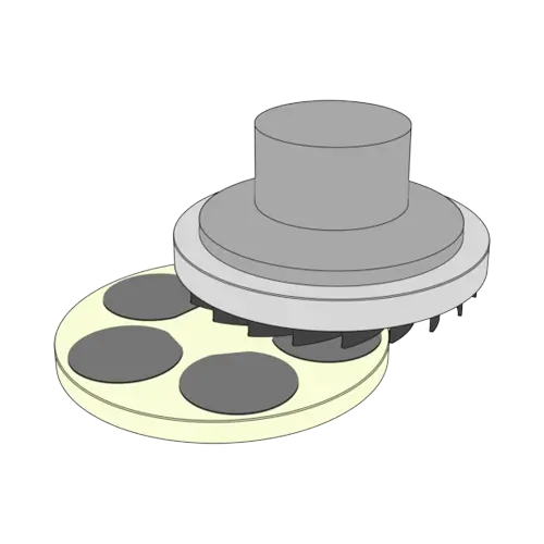
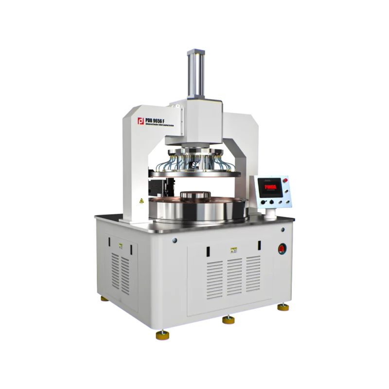
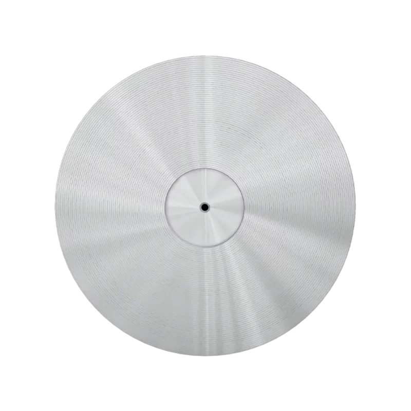
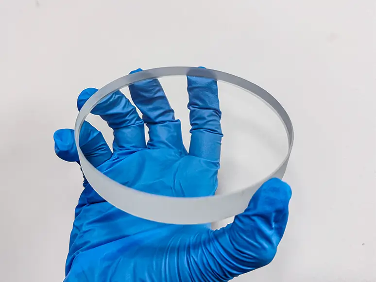
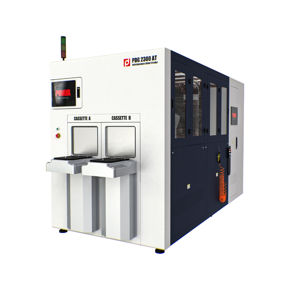
Wafering
In semiconductor manufacturing, users require thinner, more uniform wafers with higher yield to be packaged into chips. Therefore, the Wafering series is specifically developed to meet these needs.
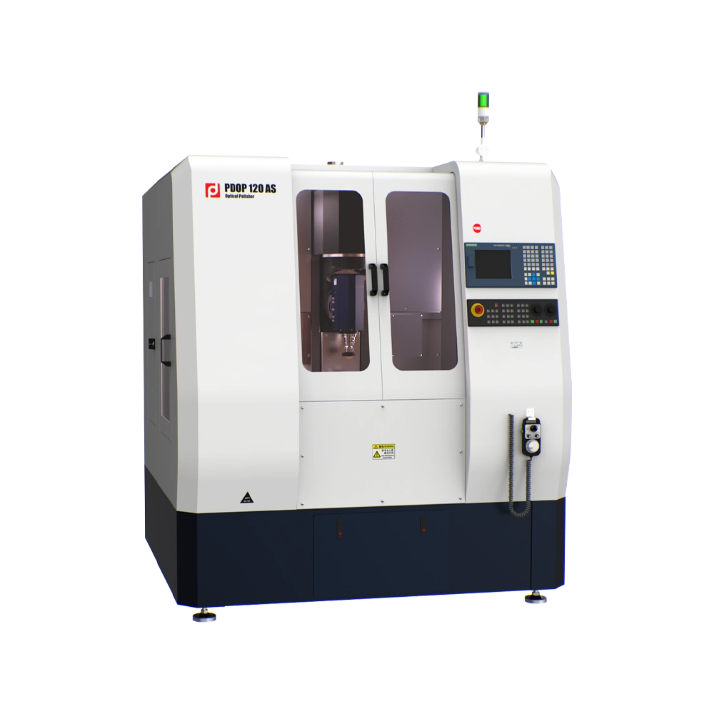
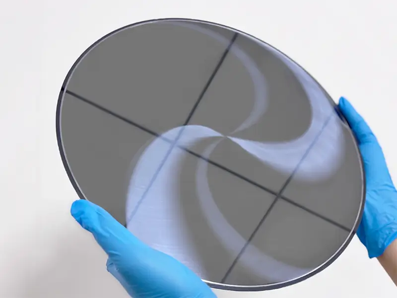
Spherical and Aspherical Processing
In optical machining, multi-axis CNC equipment is usually required to process spherical or aspherical lenses in order to achieve ultra-precise control over the shape of the workpiece.
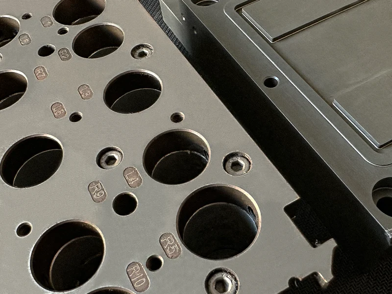
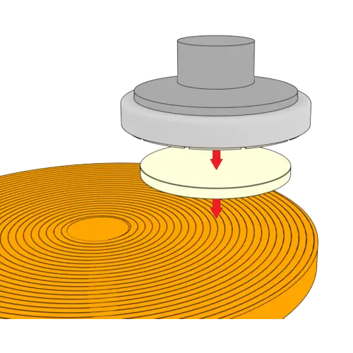
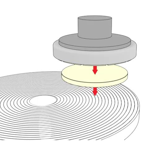
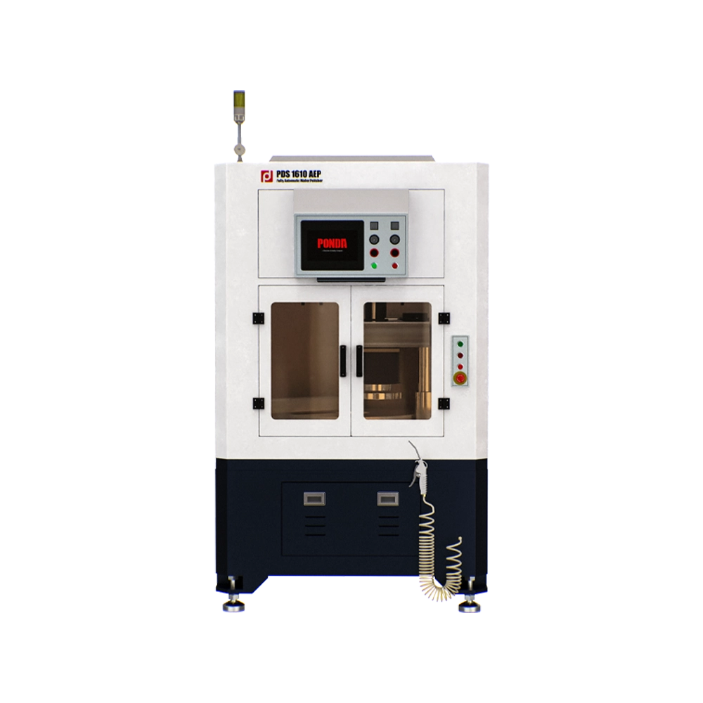
Flat Finishing
Products like static-pressure bearing and linear slider, high-precision optical lens, sealing valve, benchmark block require flat finishing equipment.
|
Wafer Manufacturing |
Wafer Fabrication |
|||||||||
|---|---|---|---|---|---|---|---|---|---|---|
|
|
» |
|
» |
|
» |
|
» |
|
» |
|
|
Ingot Slicing |
Chamfering |
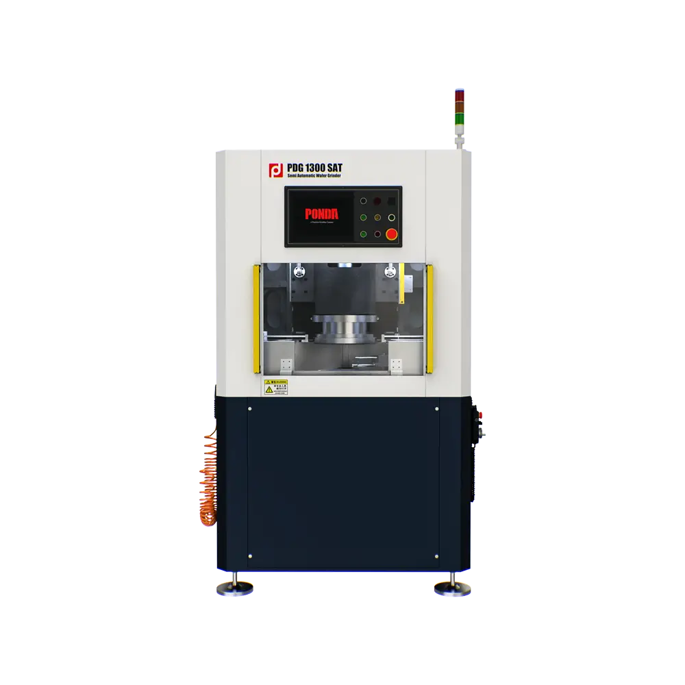
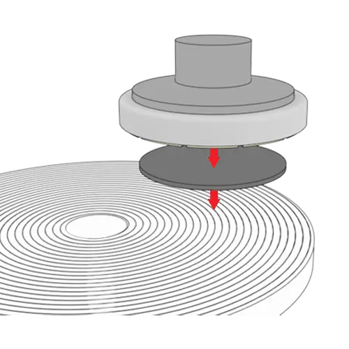
Grinding |
Patterned Wafer |
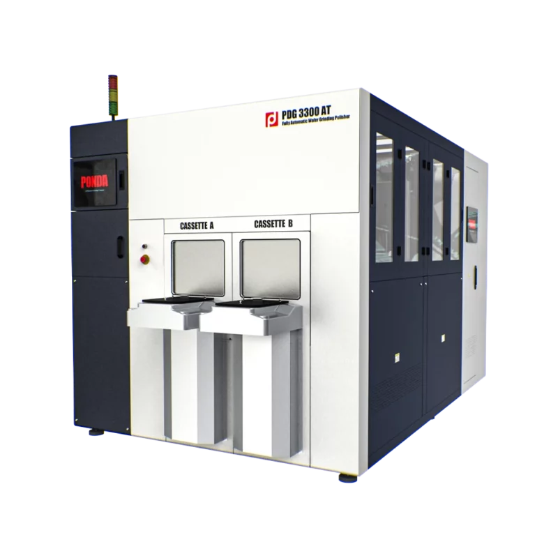
Backgrinding |
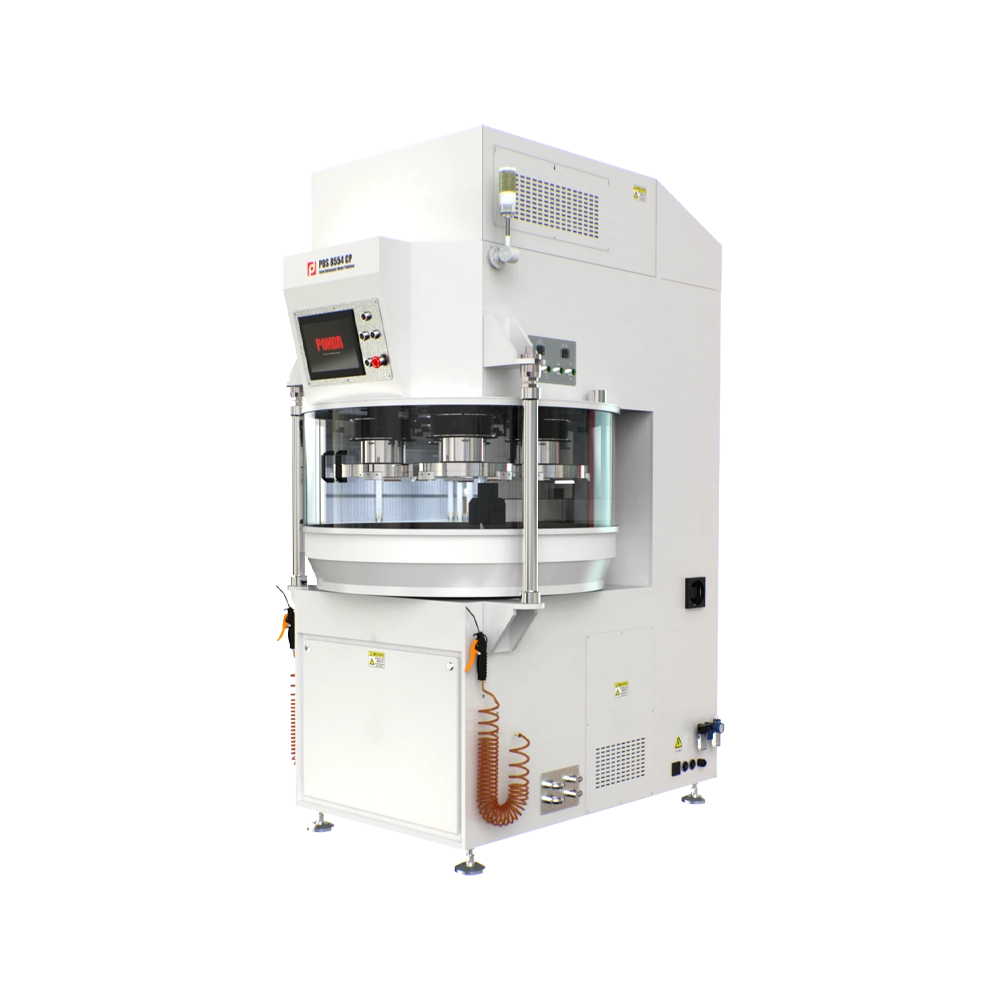
CMP Finishing |
|||||
|
|
|
|
|
|||||||
|
⬇︎ |
⬇︎ |
⬇︎ |
⬇︎ |
|||||||
|
Sapphire, GaN Manufacturing |
Lapping & Polishing |
Wafering Fabrication |
||||||||
|---|---|---|---|---|---|---|---|---|---|---|
|
|
» |
|
» |
|
» |
|
» |
|
» |
|
|
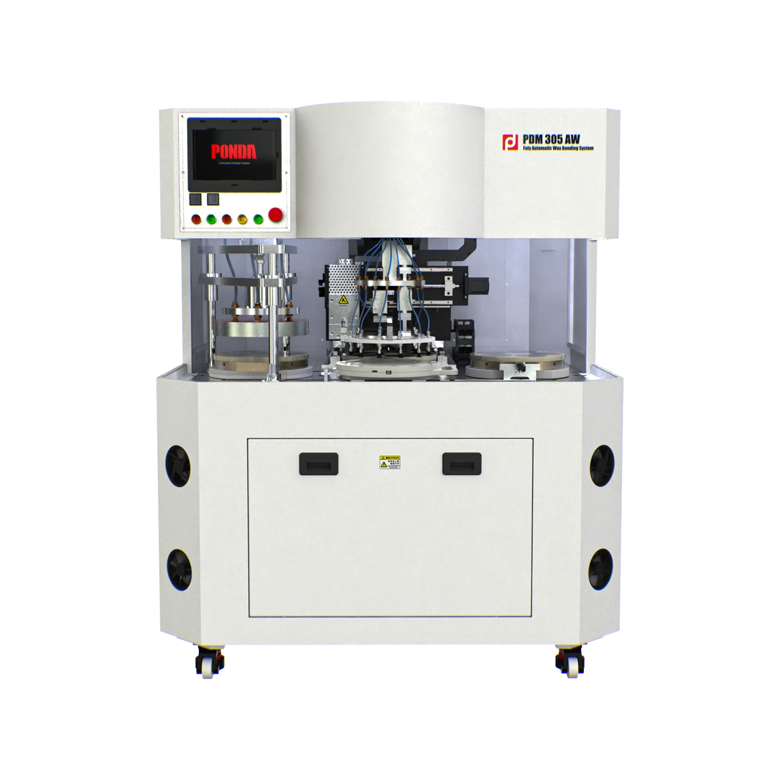
Wax Bonding |
Grinding |
Patterned Wafer |
CMP Finishing |
Backgrinding |
CMP Finishing |
|||||
|
|
|
|
|
|
|
|||||
|
⬇︎ |
⬇︎ |
⬇︎ |
⬇︎ |
⬇︎ |
||||||